| |
 |
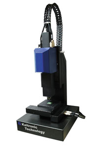
KIP 3D Inspection Equipement |
|
|
| |
Features: |
|
| |
| |
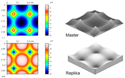
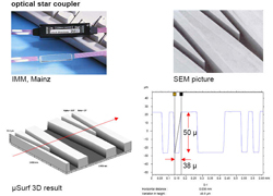
KIP 3D inspection is a 3D surface profilemeterimage scanning machine. Apply to PCB、WAFER、MEMS、IC-PACKAGING、MLCC、SOLAR BATTERY COATING、SOLDER BUMP、SMART CARD industries. KIP Ⅲ can precisely measure the topography, contour, roughness, tilting, coating, co-planarity of object, which allows you to control the stability of your production. You may use it in the laboratory and medical research. Furthermore the set-up time is very short and the operation is handy, it’s your best partner for quality assurance. | |
|
| |
|
|
| |
 |
|
Resolution: |
X/Y: 0.3um, Z: 0.001um |
|
Speed: |
10-15 second/ check point |
|
Criteria: |
Criteria 3D image, Topography, 2D profile, Via hole depth/width, Line/space width/height, warpage, roughness, co-planarity, straightness, flatness....
X/Y range |
|
X/Y range: |
510 x 610 mm |
|
Z depth: |
350 μmm | | |
|
| |
|
|
| |
|
|
| |
|
|
| |
|
|
| |
|
|
| |
|
|
 |
| |
KAITRONIC TECHNOLOGY CO., LTD. |
|
| |
Add:No.870, Sec. 3, Xinsheng Rd., Zhongli City, Taoyuan County 320, Taiwan |
|
| E-mail:mailto:service@kaitronic.com |
| |
TEL:+886-3-453-3569│FAX:+886-3-453-2113 |
| | |
 |